Featured Article

Combining imaging capabilities for high-resolution spatial and chemical characteristics
To understand the properties of a material, scientists often examine it with an electron microscope, sometimes using different levels of magnification. It can also be useful to combine similar imaging techniques that can distinguish details of the sample for comparison, and that’s what scientists get from S/TEM—a platform that allows materials to be imaged with transmission electron microscopy (TEM) and scanning TEM. “TEM blasts high-energy electrons through the sample to get information about the internal structure of the material,” says Thomas Isabell, director of the TEM product division at JEOL USA (Peabody, Mass.). “STEM focuses electrons to a fine point and scans them across the sample.” This combination of imaging modalities provides new opportunities. “You usually just have TEM or STEM,” says Brian Van Devener, surface scientist at the University of Utah’s Surface Analysis and Nano-Scale Imaging Lab in Salt Lake City, “but S/TEM can be operated in either mode.”
The option to use TEM or STEM offers greater flexibility. “Having the capability to do both in one instrument provides a robust tool,” says Van Devener. “You don’t always know which mode will give you the information that you need the most.” So a scientist can image a sample in TEM or STEM, all without moving the sample between different instruments.
“S/TEM can provide critical information—images, chemical spectra, mechanical, electrical, magnetic, structural—about a very wide variety of materials from the micron scale right down to the sub-atomic scale,” says David Foord, director of marketing at FEI (Hillsboro, Ore.). “The range of applications is pretty diverse,” Van Devener says. Chemists, engineers, material scientists and biologists benefit from the versatility of this dual-mode technology.
Seeing the never seen
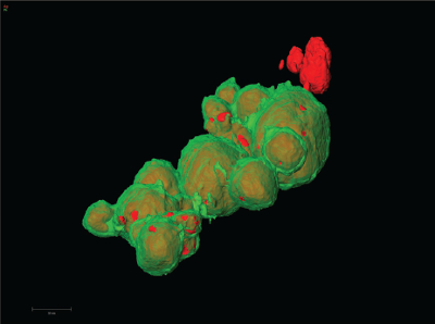 Three-dimensional EDS tomography of silver-platinum core-shell nanoparticles. The silver cores are shown in the false color of red, covered by green-colored silver shells, only a few nanometers in thickness. This tomography makes visible the pores that partially expose the cores. (Sample courtesy of Professors Yi Ding and Jun Luo, Center for Electron Microscopy, Institute for New Energy Materials and Low-Carbon Technologies, School of Materials Science and Engineering, Tianjin University of Technology, China. Image courtesy of FEI.)
This combined platform helps scientists see and understand things that they could not without it. At the University of Utah, Zak Fang, professor of metallurgical engineering, used S/TEM to explore hydrogen storage in magnesium hydride, says Van Devener. With this material, a transition- metal catalyst drives the cycle from hydrogenated to dehydrogenated, which allows the storage and release of energy. Fang wanted to see if the transition metals lie on the surface or inside the material. Van Devener combined energy-dispersive spectrometry (EDS) with S/TEM, but he still needed more. So he collected imaging data, tilted the sample and collected data again and continued this process. He then combined the data tomographically to get a 3-D image. “We showed that after successive hydrogenation/dehydrogenation cycles, the transition metals move toward the surface,” Van Devener explains. “This verified some theoretical predictions from Fang’s group and complemented some other work that showed that these metals move to the surface.”
 S/TEM-HAADF (high-angle annular darkfield) image of a palladium–rhodium bi-metallic nanoparticle during the early stages of its formation. The five distinct regions are indicative of its fivefold rotational symmetry, colorized for easy viewing. (Image courtesy of Moon Kim’s group [Ning Lu, Jinguo Wang], University of Texas at Dallas. Sample provided by Younan Xia, Georgia Tech, Atlanta.)
By adding capabilities such as EDS, scientists can get even more from this platform. “Spectroscopic capabilities like EDS show you the elemental distribution in materials,” Van Devener explains. “Crystallographic techniques can also be used to get direct crystallography at small scales, and other accessories are available, too.” So the breadth of an S/TEM can be expanded with add-on technology, and the range depends on the instrument being used.
Adding new options
As this technology advances, more features enhance the images. Using a smaller probe focuses electrons on a finer point. Combining that with an improved detector improves the resolution. Isabell says that such advances make a platform that is “more efficient at exploring a material’s chemistry.”
The high-resolution of S/TEM lets scientists explore materials in new ways. As Foord points out, “S/TEM reveals sub-nanometer material defects or distribution of strengthening or weakening mechanisms, such as precipitates, grain boundaries or dislocations, which are atomic level–local rearrangements of atoms that can be either advantageous or detrimental to a material’s properties depending on the material or use case.”
Such close examination allows scientists to design and make new materials and then analyze the structure to see if it came out as expected and if the material behaves as desired. If not, scientists can use the information from S/TEM to figure out what went wrong and how to fix it.
A team from Oak Ridge National Laboratory (Oak Ridge, Tenn.) and the University of California San Diego used STEM to study lithium-ion batteries.1 The authors noted: “Lithium-ion batteries are a leading candidate for electric vehicle and smart grid applications. However, further optimizations of the energy/power density, coulombic efficiency and cycle life are still needed, and this requires a thorough understanding of the dynamic evolution of each component and their synergistic behaviors during battery operation.” By exploring the structure and chemistry at the atomic level with this technology, they concluded: “[Many] of the previously formidable tasks, such as visualizing the distribution of light elements, unraveling the interface structure and chemistry at the atomic scale, probing the [solid-electrolyte interface] layers and so on, are now achievable.”
S/TEM technology promises even more advanced applications. At FEI, says Foord, new technology allows “more sensitive experiments over longer time periods, such as large-area chemical mapping and 3-D imaging and chemical tomography.” He adds that advances in EDS X-ray detection provide “fast chemical mapping to increase throughput for our industrial customers that may have to control industrial processes by characterizing manufactured structures at the near atomic level.”
Getting up to speed
It takes some operator knowledge to use an S/TEM, says Van Devener, especially to switch between modes. “This is something that you’d learn by a course instead of a quick standard operating procedure,” he says. “Once trained, it’s not difficult to switch between modes, and it usually takes only a couple [of] minutes.” The University of Utah runs a seven-week course on using S/TEM, and other universities offer similar training.
Sample preparation requires training, too. “When looking at the atomic level,” says Isabell, “the sample has to be prepared very well. There are a lot of techniques to do that.” Some institutions, including Stanford University, offer special training in sample preparation for S/TEM.
Getting the preparation right and then combining it with S/TEM offers new opportunities for scientists interested in the characteristics of a material. As Van Devener concludes, “It’s a powerhouse of an instrument.”
Reference
- Qian, D.; Ma, C. et al. Advanced analytical electron microscopy for lithium-ion batteries. NPG Asia Materials 2015, 7, e193.
Mike May is a freelance writer and editor living in Ohio. He can be reached at [email protected].