Featured Article

Nanoscale—or smaller—structures plus other features of materials can be analyzed with today’s technology
It’s not just what you can see in microscopy, but what you can touch and feel. In the early 1980s, two new kids on the imaging block—atomic force microscopy (AFM) and scanning tunneling microscopy (STM)—enabled exactly that. These techniques, known in combination as scanning probe microscopy (SPM), use a probe, position sensors, and extensive signal-processing instrumentation to precisely feel their way around a sample. Briefly, the probe interacts with a surface, and instrumentation records the data on interaction strength, such as the force on the probe or the current flowing between the probe and the surface. From such data, scientists can determine and view a material’s topology, structure, and composition—often at the nano- or even atomic scale.
In an excellent review of the field,1 Sergei V. Kalinin, director of the Institute for Functional Imaging of Materials2 at Oak Ridge National Laboratory in Tennessee, and his colleagues wrote that “the relatively low cost and ease of use of SPMs made them the workhorse of nanoscience.” Today, scientists use SPM to analyze and control materials—sometimes, atom by atom.
“Advances in this technology can do fascinating things,” says Thomas Mueller, director of product management at Bruker Nano Surfaces (Santa Barbara, CA). “AFM is used extensively for electrical characterization in such hot fields as batteries, semiconductors, and energy research, including studies of organic photovoltaics.”
Exploring electromechanics
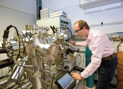 At the Institute for Functional Imaging of Materials at Oak Ridge National Laboratory in Tennessee, Sergei V. Kalinin and his colleagues apply scanning probe microscopy to many problems and develop new ways to share data. (Image courtesy of Oak Ridge National Laboratory, U.S. Department of Energy.)
Often in science, new technologies can bring a fresh perspective to well-studied fields, and that is the case with SPM and electromechanics. In the 18th century, Italian natural philosopher Luigi Galvani made muscles twitch in dead frogs by stimulating them with electricity—that is, an electrical input created a mechanical output. This observation was one of the most seminal moments in the history of physics, giving rise to the modern theory of electricity and entering modern language (“galvanize”). It is also the first known example of an electromechanical study.
Over the centuries, many other biologists explored the world with reactions to electricity—often on increasingly fine scales. Rather than bluntly stimulating a frog leg, neuroscientists developed tools to inject current into single nerve cells and then record the outcome, such as triggering contraction in specific muscles. However, in the world of physics, electromechanics remained less explored and was confined mostly to the relatively small subset of materials known as piezoelectrics, since large voltages are necessary to produce a measurable response. For example, thousands of volts need to be applied to a piece of quartz to make it expand or contract by even two nanometers.
 SPM can reveal the structure of many samples, such as boron nitride, shown here. (Image courtesy of Oak Ridge National Laboratory, U.S. Department of Energy.)
With SPM, the measurable scale dips deep into the nanoworld. In describing electromechanics, Kalinin says, “The effect is widespread—almost all materials have some electromechanical coupling, but it’s usually very weak.” For example, applying one volt to a material might create one picometer of deformation, which is one-billionth of a meter or about one-twentieth of the diameter of a hydrogen atom. That’s not much movement, but Kalinin says electromechanics is very strongly related to properties of the material, such as the orientation of the crystalline axes or how atoms move in it.
This phenomenon can also be used to great effect in modern applications, such as the molecular machines that earned Jean-Pierre Sauvage (University of Strasbourg, France), Sir J. Fraser Stoddart (Northwestern University, Evanston, IL), and Bernard Feringa (University of Groningen, The Netherlands) the Nobel Prize in Chemistry 2016. While these machines can be synthesized, SPM opens the pathway to probe them one by one and potentially assemble them in more complex structures.
Tapping into new applications
Recently a lot of progress has been made in understanding how an AFM interacts with a sample, and that impacts what can be measured. Newer technology, such as Bruker’s PeakForce Tapping mode, simply put, can explore materials at high resolution without damaging the surface. As an example, Mueller mentions that scientists from Brown University (Providence, RI) and General Motors (Detroit, MI) worked with Bruker to study lithium-ion batteries.3 “AFM with PeakForce Tapping was used to look at the solid electrolyte interphase—SEI layer—above a silicon anode,” Mueller says. This surface is very soft, and is typically damaged by other SPM modes. Nonetheless, these scientists explored the surface in situ and in operando at the nanoscale, and revealed cracking that helps explain the key issue of battery degradation. With this imaging technology, scientists can correlate a battery’s efficiency with its structure and how that structure changes from charging and discharging—helping them work toward longer-lifetime, higher-capacity batteries.
In addition, different energy applications can require different capabilities of AFM. For example, scientists studying artificial photosynthesis make measurements in liquid. For this, Bruker developed AFM probes that are insulated at all points except the tip.4 “A very small tip sticks out and gets much better than 100-nanometer spatial resolution in scanning electrochemical—SECM—measurements,” Mueller says. With this probe, scientists can measure conductivity just above the surface of a material or touch the surface with PeakForce Tapping to measure the contact current. “One of the strengths of AFM is the ability to work in situ,” Mueller says. “With this probe and PeakForce Tapping, one can do new in situ functional studies of photocatalysis, fuel cells, batteries, but also biosensors and other devices.” He adds, “It’s a vast range of opportunities.”
Big data from small structures
“The rest of the world is changing dramatically—using Google Scholar and Facebook—but in science we use the same scope and searches that we used five years ago,” Kalinin says. The sharing of information among people is not being replicated in data from microscopes.
Kalinin realizes the limitations of a single person analyzing information. The data from his microscope goes to his computer, where he analyzes the results. “But, I only analyze [a] fraction of data collected,” he says, “and the conclusions can be limited by my expectations and experience.” To get more from that data, Kalinin wants to make it available to more eyes and minds. There’s a lot of data to share, because an SPM can generate 10 gigabytes in 10 minutes. So, his team is learning how to capture the full stream of data and make it available to other scientists. “We’re going from small-data microscopy to big-data microscopy,” he says. “We don’t always need all of the data, but we would not know that a priori.” The tools that Kalinin and his colleagues developed—deployed via GitHub on the web— and associated YouTube training videos are available for free.6 These tools can even be customized by scientists for specific applications.
Viewing in a vacuum
The first SPMs operated in a vacuum, and some still do. Scienta Omicron (Taunusstein, Germany) makes SPM platforms that work in an ultrahigh vacuum—like 10-10 torr—to keep samples clean and enable work at liquid- helium temperatures. With these capabilities researchers can study fundamental electronic structures of materials. “A contaminant-free sample is essential for a good experiment, and the lower the temperature, the lower the thermal noise contribution to the data,” says David Laken, sales manager at Scienta Omicron. “Plus, at low temperatures, your molecule of interest can be frozen to the surface for study.”
Such low temperatures can be very costly to produce, because liquid helium is expensive. In a 4He system, it costs about $1000 per dose of the coolant. Scienta Omicron offers platforms that are cryogen-free. “There have been cryogen-free coolers for some time,” says Laken, “but as the cooling process uses mechanical pumps, generating disruptive mechanical vibrations, they have not been able to be effectively combined with SPMs until recently.”
Since the early days, SPM systems have been used to move individual atoms. According to Laken, “Leading researchers use our systems to create single-atom qubits,” which can be used as the computing units of a quantum computers.
It’s a long way from stimulating a frog’s legs to building a quantum computer, but science often connects unexpected phenomena. Today’s connections between atomic structures and teeny movements would surely amaze Galvani, and the result is a continuing march toward greater discoveries, technologies, and consumer products.
References
- Kalinin, S.V.; Strelcov, E. et al. Big, deep, and smart data in scanning probe microscopy. ACS Nano 2016; doi: 10.1021/acsnano.6b04212.
- http://ifim.ornl.gov/
- Kumar, R.; Tokranov, A. et al. In situ and operando investigations of failure mechanisms of the solid electrolyte interphase on silicon electrodes. ACS Energy Letters 2016; doi: 10.1021/acsenergylett.6b00284.
- Desbief, S.; Dubois, P. et al. Nanoscale investigation of the electrical properties in semiconductor polymer-carbon nanotube hybrid materials. Nanoscale 2012; doi: 10.1039/c2nr11888b.
- Nellist, M.R.; Chen, Y. et al. Atomic force microscopy with nanoelectrode tips for high resolution electrochemical, nanoadhesion and nanoelectrical imaging. Nanotechnology 2017; doi:10.1088/1361- 6528/aa5839.
- http://ifim.ornl.gov/resources.html
Mike May is a freelance writer and editor living in Florida. He can be reached at [email protected].