Featured Article

Please see our Scanning Electron Microscopes (SEM) section to find manufacturers that sell these products
Centuries ago, glass lenses were employed to visually enhance small objects beyond the physical ability of the human eye. Light and compound microscopes led to the birth of microbiology. However, the physical properties of visible light greatly limited the resolving power of optical microscopes.
In the first half of the twentieth century, great leaps in resolving power were made possible by experimentation with applied electron beams, resulting in the visualization of matter at <10 nm. Excitation of electrons on the surface of a material via electron beam resulted in a scattering of secondary electrons, the pattern of which formed the image generated as an electron micrograph. With the advent of electron microscopy, physicists set on a quest to visualize the atomic world.
Several physicists began investigating the creation of a stable electron microscope image. In 1937, Manfred Ardenne characterized the intricacies of using electron probes for scanning materials with an electron beam, for the most part by the manipulation and amplification of a specific current. His work became the springboard for the perfection of scanning electron microscopy (SEM).
Mid-twentieth century: the nascent SEM market
The Japan Electron Optics Laboratory, or JEOL, was formed in Japan in 1939 to research and expand the applications of EM technology. Carl Zeiss, Philips and Siemens were researching EM technology on the European front. Globally, for the next two decades, many independent researchers and academic institutions were trying to perfect a reliable SEM. Stereoscan, the world’s first-ever commercial SEM instrument, was marketed by Cambridge Instrument Company; the first Stereoscan, a prototype, arrived at Dupont Chemical Corporation in 1965.
Since the initial commercialization of SEM, improvements in electron beam sources, signal detectors and computer interfaces have expanded the sensitivity and application of the technology. SEM technology has become useful in many fields, among them archaeology, biology, materials analysis, geology, medicine, semiconductors and pharmaceuticals. Purpose-built, durable SEM equipment is utilized by the engineering and petroleum industries. The range of sample types that can be analyzed with SEM technology has continued to expand along with the fields in which it is used.
Today’s instruments are more user-friendly than the earliest renditions, and now, excellent SEM imaging is accessible: in the lab, on the benchtop or out in the field. According to Vern Robertson, SEM specialist at JEOL (Peabody, Mass.), “In the early days, instruments were cumbersome, confined to a dedicated lab space and used a limited suite of detectors. Now, SEM technology is used for analysis of semiconductors, biological specimens, and more. Many instruments have multiple imaging detectors and spectrometers built in as standard.”
Scanning electron microscope purchasing considerations
Selecting an SEM technology for a laboratory begins with defining the type and/or range of samples that will be analyzed. Prospective users can consider the desired range of magnification, specimen stage, instrument size and image output. These parameters will help the user decide between an entry-level benchtop SEM, a lab workhorse SEM or an ultrahigh-resolution field-emissions gun (FEG) SEM.
Years ago, laboratories required a dedicated microscopist, an operator with many years of experience to run SEM instruments. Now, the instruments operate in multiuser facilities, where they are regarded as another tool in the toolbox, along with FTIR, optical microscopy and other imaging modalities.
Typically, SEM imaging is considered when more than simple morphological characterization is needed, or when in-depth imaging, such as elemental composition and chemical state analyses, is required. Modern systems also offer correlative microscopy options that combine SEM and optical imaging, or add X-ray analysis/energy-dispersive X-ray spectroscopy (EDS, EDX or XEDS) and/or additional detectors. Advances in detector technology, such as in-column detectors and deceleration of the beam in the column and/or at the sample, provide for extremely high resolution.
Imaging a variety of samples
Environmental SEM (ESEM) and variable-pressure SEM (VPSEM) technology, which have been used for some time, do not offer resolution equal to that of field-emission SEM (FESEM). These higher resolutions are particularly important to scientists looking to examine hydrated biological samples, who typically prepare samples cryogenically. Cryo-transfer, or cryogenic treatment, is more accessible and simpler than ever. For example, a cryo-transfer system can be attached to an SEM microscope: it allows the user to freeze-plunge the sample, freeze it rapidly, fracture it open, etch it and coat it, in situ. Cell biologists, for example, benefit from the superior resolution provided by FESEM and the use of cryogenic sample preparation, which eliminates the need to coat samples.
ESEM allows for more dynamic experiments: users can thoroughly observe the progression of chemical activity within a sample. Most buyers of ESEM technology operate in low-vacuum modes. For example, diaper manufacturers utilize ESEM to monitor the dynamics of a test diaper: they wet it, watch it swell and analyze the pattern of water distribution and its effects on the fabric by tracing the activity of the water vapor. To add another real-life example: researchers can literally watch paint dry with ESEM, by observing the behavior of latex beads on a surface,
Imaging samples that cannot be processed or coated
 An example of the size of SEM instruments in the 1970s. Pictured is JEOL’s JSM-35CF. (Image courtesy of JEOL USA.)
If chemical fixation or cryo-fixation cannot be used on a delicate sample, a low-vacuum SEM/low-vac SEM is the ideal choice for quick analysis. The most common usage is imaging and analysis of any sample that is nonconductive, cannot be coated, is not high vacuum compatible or is in some state of hydration, e.g., ceramics, glass, biologicals, corrosion, polymers, forensics, etc. These SEMs can also be run in a traditional highvacuum mode.
An example of a VPSEM that is capable of measuring relatively large, unprocessed biological samples up to 300 mm in diameter is the Hitachi S-3700N Ultra Large VP-SEM (Hitachi High Technologies America, Schaumberg, Ill.). The S-3700N enables users to perform nonconductive sample imaging on raw biological specimens such as organs.
If a variety of samples are to be analyzed, which may include an assortment of biological, dehydrated, solid or conductive samples, combined instruments such as those in FEI’s Quanta line (FEI, Hillsboro, Ore.) offer the versatility of conventional SEM combined with VPSEM and ESEM.
SEM imaging of solid materials
Conventional SEM imaging is best suited for the analysis of solid, conductive materials, primarily for materials engineering, geology, chemistry and industry. Refer to Table 1 for more detailed subtypes of SEM and combined SEM technologies.
Table 1 – SEM instruments: types, features, industries and applications
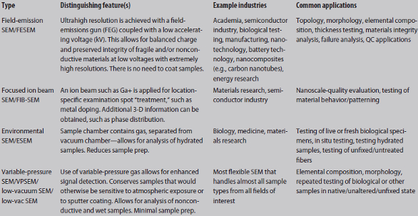
A conventional SEM instrument can be equipped with EDS detectors to measure X-rays generated by the electron beam for elemental analysis. Instruments range in size from desktop applications to large units. An example of a smaller benchtop instrument that can measure the different elements within a sample utilizing EDS is the Phenom ProX Desktop Scanning Electron Microscope from Phenom-World (Eindhoven, The Netherlands).
A versatile FIB-SEM instrument is ideal for the user seeking in-depth 3-D information such as phase distribution. Paired with traditional SEM, FIB technology allows for nanotomography, failure analysis and nanoprototyping because surfaces can be etched or manipulated with the use of ion beams. An example of a combined FIB-SEM is the TESCAN LYRA 3 XM FIB-FESEM (Tescan USA, Inc., Warrendale, Penn.), which features a high-resolution Schottky FEG-SEM column and an extra-large XM chamber with a stage capable of accommodating large samples. LYRA 3 XM features numerous interface ports with optimized analytical geometry for EDX, wavelength dispersive X-ray (WDX) and electron backscatter diffraction (EBSD), as well as the capacity to attach many other detectors.
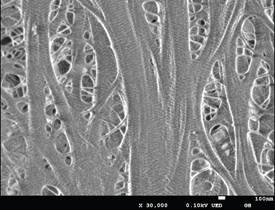 An uncoated polymer battery separator imaged at 30,000× utilizing a 0.1- kV GB mode upper electron detector (UED). (Image courtesy of JEOL USA.)
Geological applications call for in-depth minerals characterization. Specialized SEM instruments such as the ZEISS Mineralogic Series (Carl Zeiss Microscopy, Peabody, Mass.) combine conventional SEM with one or more EDS detectors to aid in the analysis of specific patterns and formations. Also, if a laboratory requires multiple SEM detectors for a variety of sample types, Bruker provides a “5-on-1” SEM analytical tool range with full integration of EDS, WDS, EBSD and micro-XRF, managed via computer with ESPRIT 2.0 software (Bruker AXS, Billerica, Mass.).
Research, analysis and rapid observation can be performed by “entry-level,” versatile, high-performance SEM devices such as JEOL’s JSM-6010PLUS/ LA, which combines EDS with a silicon drift detector (SDD). The device offers high performance at an entry-level price and features backscatter detection, low-vacuum and high-vacuum modes, a five-axis stage and a multi-touchscreen interface.
X-ray/EDS detectors have been around since the late 1960s. However, they presented several limitations: they required the use of liquid nitrogen for cooling, were generally small (10 mm was standard for decades, and that size does not allow for many X-ray counts) and, if a sample could not tolerate a lot of X-ray counts, the detector could only process several thousand counts per second without a degradation of performance.
Silicon drift detectors are passively cooled, eliminating the need for liquid nitrogen. Physically, there is no anode on the front and back: it is a set of thin, semiconcentric rings. Lending to their physical design, SSDs handle more counts per unit time, and are much larger and faster than standard EDS detectors. The same amount of data can be obtained 10 times faster, and a user can “back down” on the beam so as not to damage the sample or cause the sample to charge.
For industrial, military, geologic and oilfield environments outside of the confines of the laboratory, instruments such as the ASPEX Extreme series (FEI) are more portable and rugged, and combine SEM imaging with fast EDS to rapidly detect the size, shape and elemental composition of samples.
SEM has far-reaching applications. For example, SEM instruments can feature hot and cold stages for examining the performance of materials during specific manufacturing practices. A sample material can be imaged while it is exposed to rapid heating and cooling, pulling and bending and performing electrical experiments, such as running a current through a sample.
Trends and highlights in the SEM realm
Correlative microscopy
The term “correlative microscopy” usually refers to the pairing of optical microscopy with SEM. By taking an image with an optical microscope, such as a stereomicroscope, a petrographic geologic microscope, confocal, fluorescent, metallograph or any other optical microscope, correlative microscopy occurs when the optical image is taken to SEM analysis. An SEM analysis of the optical image is performed; then the two are overlaid. The superimposed image allows for rich, positional data.
Any researcher who has paired SEM with X-ray spectroscopy has already performed correlative microscopy by combining two different detectors and two different types of signals. By utilizing two different techniques to create an elemental map over an image, correlative microscopy permits the analysis of both the chemistry and chemical distribution found by imaging a sample.
SEM microscopes navigating optical images
Many high-end optical microscopes feature motorized stages. The x,y coordinates of the stage are stored within a text file or the header information of the image. That data can then be read by the SEM software, which navigates to the same location on the sample image to create precise correlations. If a user has an optical microscope without a motorized stage, software such as that offered by JEOL allows for correction of magnification and rotation. A user is able to “point and shoot” on the optical sample image, then navigate to the desired location on it. Therefore, even an image taken with an unmotorized optical microscope can be overlaid for SEM analysis.
SEM image montage
Many SEM users want the ability to montage, or be able to take a sample and image it entirely in automated, traceable fashion. Modern software enables the acquisition of large, terabyte-sized images by automatically setting the stage for best acquisition of individual images, typically at a low magnification. The separate images are stitched together. At the end of the cycle, hundreds of small images are stitched together to create one image, or montage.
The primary benefit of an image montage is the quality of the detail obtained. Examples of ideal candidates for a montage include an integrated circuit, a complete failure part or a geologic cross-section. Images can then be digitally zoomed with no pixelization. Semiconductor researchers can better perform reverse engineering or failure analysis utilizing an image montage. A geologist might use an image montage to map out an entire thin section of a sample, for example: a 20-mm × 55-mm section, analyzed for its X-ray chemistry distribution. X-ray spectrometers are limited to the lowest magnification at which they can work, which is typically 50–500×. At 50×, acquiring an image with X-ray data of an entire geological thin section might take hundreds of images, in which case a montage is indispensable.
A variety of SEM sample preparation tools for time savings
Generally, there are two categories of sample preparation tools for SEM instruments. The first embodies some form of coater to apply regular metal, sputtered metal, evaporated metal and evaporated carbon coatings. The second category of preparation comprises tools for thoroughly cleaning samples. Surface sensitivity increases when higher magnification and lower voltages are utilized. Therefore, hydrocarbon contamination from polishing or handling can hinder the ability to perform high-resolution imaging. SEM users might consider purchasing ozone or plasma cleaners to clean their sample. Another example of an SEM sample preparation tool is a cross-section ion-beam sample polisher. It employs a defocused ion beam to make polished cross-sections and utilizes an argon ion rather than gallium, eliminating gallium implantation and the potential for heavy ion damage. Because the argon ion beam in the sample polisher is defocused, it is not completely concentrated into a localized area.
Data output, software
The basic operational software of SEM microscopes is typically written by the vendor and is hardware specific. The graphical interface is proprietary. X-ray maps and spectral data are converted to a standard, shareable file format and can then be exported to MSA or PNG file formats without much difficulty. The images are typically of .BMP, .TIFF, or .JPG/.JPEG file formats. Images and data can be easily be dropped into Word, Powerpoint, or Excel, or converted to PDF.
Researching and buying SEM instruments
The comprehensive directory available at labcompare.com enables scientists to research, compare and contrast SEM instruments from many major manufacturers. Many if not all vendors make instruments that fit all of the examples mentioned above. After comparing specifications, users are able to submit their information to receive price quotes, directly from the instrument manufacturer.
SEM imaging contest
For 2015, JEOL is continuing its monthly SEM imaging contest. Users of JEOL instruments are invited to apply at the company’s website for the chance to win a $100 Amazon gift card in a monthly drawing. At the end of the year, grand prize winners from the areas of biological or materials research will be selected for two $300 grand prizes.
Emilia Raszkiewicz is managing editor, American Laboratory; [email protected]. American Laboratory would like to thank Vern Robertson, SEM specialist and technical sales manager at JEOL USA, for contributing his expertise to this article.
Please see our Scanning Electron Microscopes (SEM) section to find manufacturers that sell these products