How Does a Scanning Electron Microscope Work?
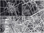
A scanning electron microscope (also commonly abbreviated as SEM) uses beams of electrons to create magnified images of samples, as opposed to beams of light that a traditional microscope uses. SEMs use electrons that are bounced off near the surface region of a sample. Because the wavelength of electrons is notably smaller than that of light, the resolution of SEMs is greatly superior to that of a light microscope.
What Are Scanning Electron Microscopes Used For?
Because the SEM can magnify a sample up to 500,000 times its normal size and determine its chemical makeup, scanning electron microscopes have a wide range of applications. They are used for quality control in both the pharmaceutical and semiconductor industries, sample comparisons in forensics, diagnostics in medical labs, and in research labs to determine the composition of samples treated in different ways.
What Types of Scanning Electron Microscopes Are There?
Scanning electron microscopes have different kinds of signal detectors available that include back-scattered electrons (for imaging), characteristic X-rays (for determining types and amounts of elements present in the sample), transmitted electrons, and cathodoluminescence. Other variations in different scanning electron microscopes include availability of low or high vacuum mode and imaging options for bright field samples and/or dark field samples.

Check out this article "Integrated SEM Workflow Creates Powerful 'Nano-lab' " to see more ways in which SEM can be a valuable tool for your lab.
Get Quote for All
Select up to 5 products from below to compare or request more information.
JEOL USA, Inc.
- Enables precise chemical bonding state analysis and compositional mapping, making it indispensable for researchers and engineers in materials science, nanotechnology, and related fields.?
- Multi-channel detection
JEOL USA, Inc.
- Inquire
- Provides outstanding SEM images and elemental analysis results in minutes
- Backscattered electron detector
JEOL USA, Inc.
- Inquire
- Inquire
- Secondary electron detector (SED),
Upper electron detector (UED),
In-lens backscattered electron detector (iBED)
JEOL USA, Inc.
- Inquire
- Compact stationary scanning electron microscope, embedded EDS, live analysis, heat-sensitive specimens, element maps
- Small area EDS detector
JEOL USA, Inc.
- Inquire
- Live analysis, simple EDS, high and low vacuum.
- Accommodates a wide variety of detectors and accessories such as: EDS, WDS, EBSD, CL, STEM, heating/cooling substages etc.
JEOL USA, Inc.
- Inquire
- High spatial resolution imaging and analysis
- Quadrant BSE
JEOL USA, Inc.
- Inquire
- Inquire
- Semiconductor type BSE detector
JEOL USA, Inc.
- Inquire
- High-resolution imaging, quantitative elemental analysis, and chemical state analysis
- Inquire
JEOL USA, Inc.
- Inquire
- Materials characterization, eds analysis, elemental analysis, SEM images
- Backscattered electron detector
Select up to 5 products from above to compare or request more information.
Tags:
Please Login or Register to Create Tags