The growing field of plasmonics aims to increase our understanding of the electromagnetic activity that occurs on the surface and at the interface between materials, potentially enabling the development of new unique nanotechnologies such as sensors and quantum devices. To truly understand plasmonic materials at the nanoscale, scientists need the ability to capture their interactions within extremely short timeframes and with extremely sensitive imaging systems. The recently established ultrafast electron microscope (UEM) at Argonne National Laboratory’s Center for Nanoscale Materials (CNM) showed it was up to the task when researchers managed to observe the unusual behavior of a gold nanoparticle at the edge of a sheet of a graphene sheet in sub-picosecond time resolution.
Argonne’s UEM can visualize phenomena in nanometer spatial resolution and in time frames of less than a trillionth of a second, making it an ideal tool for observing surface plasmons on nanoparticles and 2D materials. The researchers’ experiment, from the excitation of the gold nanoparticle to detection of the plasmonic field by photo-induced near-field electron microscopy via the ultrafast system, occurred in less than a few hundred femtoseconds.
The investigation revealed that although the gold particle’s plasmonic field was symmetric when sitting on the surface of a flat graphene sheet, the field became asymmetric when the particle was in close proximity to a graphene edge, becoming concentrated much more strongly near the edge region. The discovery of this unusual coupling mechanism has implications for plasmonic technology, showing how localized electromagnetic fields could potentially be manipulated. This research was published in Nano Letters.
“It’s a remarkable new way of thinking about how we can manipulate charge in the form of a plasmonic field and other phenomena using light at the nanoscale,” said Argonne nanoscientist Haihua Liu. “With ultrafast capabilities, there’s no telling what we might see as we tweak different materials and their properties.”
Plasmonic devices could be useful in a wide range of applications, from quantum information processing to optoelectronics and sensors for biological and medical purposes. The UEM system at CNM could help accelerate this growing field due to its sensitive capabilities and open user access for scientists within the Department of Energy’s Nanoscale Science Research Centers.
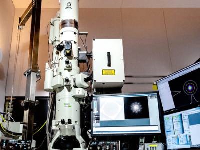
Photo: Ultrafast electron microscope at Argonne's Center for Nanoscale Materials. Credit: Argonne National Laboratory