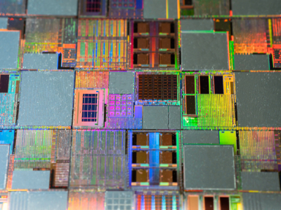
Bilkent University researchers have developed an innovative technique to enable the controlled fabrication of nanostructures within a silicon wafer with unprecedented control.
The research, published in Nature Communications, describes how the team overcame complex optical effects and diffraction limits of lasers by employing a special laser pulse. Created using spatial light modulation, the laser pulse avoids the optical scattering effects that have so far hindered precision energy deposition.
"Our approach is based on localizing the energy of the laser pulse within a semiconductor material to an extremely small volume, such that one can exploit emergent field enhancement effects analogous to those in plasmonics. This leads to sub-wavelength and multi-dimensional control directly inside the material," explained Prof. Tokel. "We can now fabricate nanophotonic elements buried in silicon, such as nanogratings with high diffraction efficiency and even spectral control."
The technique developed by the team could have a significant impact on the development of nano-scale systems with unique architectures. "Our findings introduce a new fabrication paradigm for silicon," said Prof. Tokel, "The ability to fabricate at the nano-scale directly inside silicon opens up a new regime, toward further integration and advanced photonics. We can now start asking whether complete three-dimensional nano-fabrication in silicon is possible. Our study is the first step in that direction."