A Scanning Transmission Electron Microscope (STEM) is a high-resolution imaging instrument that combines features of both SEM and TEM to provide detailed structural and compositional analysis at the atomic scale. STEM microscopes are widely used in materials science, nanotechnology, and life sciences for their ability to perform high-resolution imaging, elemental mapping, and crystallographic analysis. When selecting a STEM system, consider resolution, detector configuration, analytical capabilities (e.g., EDS, EELS), and sample compatibility. Investing in a high-performance STEM microscope enables advanced nanoscale characterization, supports cutting-edge research, and accelerates innovation across scientific fields.
|  |  |  |  | 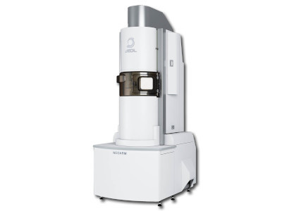 |
| Company | JEOL USA, Inc. | JEOL USA, Inc. | JEOL USA, Inc. | JEOL USA, Inc. | JEOL USA, Inc. |
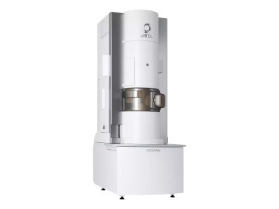
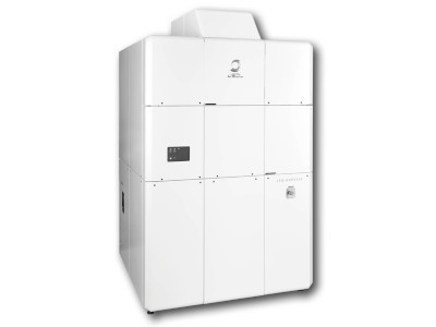
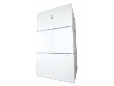
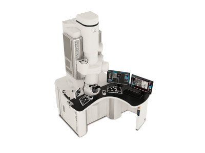
| Item | Monochromated ARM200F | JEM-ACE200F High Throughput Analytical Electron Microscope | JEM-ARM300F2 GRAND ARM Atomic Resolution Transmission Electron Microscope | JEM-F200 Multipurpose Analytical S/TEM | NeoARM Atomic Resolution Microscope |
| Catalog Number | Monochromated ARM200F | JEM-ACE200F | JEM-ARM300F2 | JEM-F200 | NeoARM |
| Price | Inquire | Inquire | Inquire | Inquire | Inquire |
| Resolution | STEM HAADF: 70 pm (200 kV), 100 pm (80 kV), 160 pm (30 kV).
TEM Information Limit: 100 pm (200 kV), 110 pm (80 kV), 250 pm (30 kV).
TEM Point-to-Point Resolution: 0.1 nm at 200 kV. | TEM Resolution: 0.10 nm (200 kV).
STEM Resolution: 0.10 nm (200 kV, with STEM Cs corrector).
STEM-HAADF Resolution: 73 pm on GaN (single frame) or 63 pm (frame accumulation). | TEM Resolution: 50 pm (lattice resolution) at 300 kV with Cs correction.
STEM Resolution: 53 pm at 300 kV, 96 pm at 80 kV with STEM corrector. | TEM resolution (at 200 kV): Point resolution - 0.19 nm to 0.23 nm Lattice resolution - 0.1 nm Information limit - ≤0.11 nm to ≤0.12 nm
STEM resolution (at 200 kV): HAADF-STEM image 0.14 nm to 0.16 nm | 0.19 nm (TEM mode) and a scanning TEM resolution of 71 pm |
| Detector(s) | Energy-Dispersive X-ray Detector (EDS): JED-2300, with a solid angle of 1.76 sr, and a resolution of 133 eV.
EELS Detector: Gatan GIF Quantum. | Dual EDS detector with SDD technology. | Optimum Bright Field STEM | large-area Silicon Drift Detector | New ABF (Annular Bright Field) detector |
| Accelerating Voltage | 30 to 200 kV | 60kV to 200kV (80 kV, 200 kV; standard, Other voltages: option) | 300kV, 80kV | 20 kV~200 kV (200 kV, 80 kV are selectable as a default. Other accelerating voltages are options.) | 30 to 200 kV (80, 200 kV : standard, 30, 60, 120 kV : optional) |
| Get Quote | Inquire | Inquire | Inquire | Inquire | Inquire |