Multispectral imaging systems are used by the food industry, the pharmaceutical industry, and in medical, biology, and chemistry labs for analysis and quality control. Types of multispectral imaging include NIR (near infrared), which can provide a quick and accurate analysis of samples within the 700–2500 nm wavelength range, and Raman, which measures the scattering of near infrared, visible, or near ultraviolet light. In both cases, the photons that are emitted and absorbed by the sample allow identification of specific molecules.
Considerations for purchasing a Multispectral Imaging System
Sensitivity, specificity, and resolution of images can vary between chemical imaging systems. Another feature to be aware of is what type of imaging the system is capable of and whether other types of imaging can be integrated into the system.
Discover and compare Multispectral Imaging Systems:
|  |  | |
| Company | Oxford Instruments | Oxford Instruments | Oxford Instruments |
| Item | TrueSurface – Topographic Raman Imaging | alphaCART – Mobile Raman System | witec360 Semiconductor Edition Raman Microscope |
| Citations | | | |
| Catalog Number | TrueSurface™ | | |
| Price | | | |
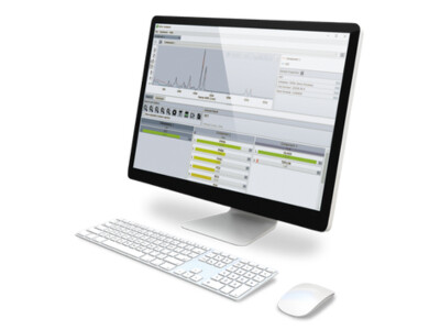
| Description | The patented TrueSurface Microscopy option for witec360 microscopes enables confocal Raman imaging guided by surface topography to maintain an optimal focus throughout a measurement.
The pioneering topographic Raman imaging technology uses an integrated optical profilometer to provide one-pass The patented TrueSurface Microscopy option for witec360 microscopes enables confocal Raman imaging guided by surface topography to maintain an optimal focus throughout a measurement.
The pioneering topographic Raman imaging technology uses an integrated optical profilometer to provide one-pass simultaneous operation.
- Enables 3D chemical characterisation of rough, inclined or irregularly shaped samples.
-
• Compensates for variations during measurements with long integration times.
-
• Features variable offset from the sample surface.
-
• Integrates seamlessly with Raman, PL, white-light microscopy.
-
• Further reduces sample preparation effort.
... Read More | alphaCART is Oxford Instruments' mobile, confocal Raman system for all applications that require bringing the lab to the sample, including specimens that don’t fit under a microscope and fragile or precious objects that can’t be removed from secure locations.
The system's high confocality and alphaCART is Oxford Instruments' mobile, confocal Raman system for all applications that require bringing the lab to the sample, including specimens that don’t fit under a microscope and fragile or precious objects that can’t be removed from secure locations.
The system's high confocality and signal sensitivity also allow measurements through protective glass and windows, which enable studies of gases or chemical processes inside reaction chambers and other enclosures.
- Freely positionable, fibre-coupled Raman probe.
- High spectral and spatial resolution, confocality, and signal sensitivity.
- Sample survey with white-light illumination and colour video camera.
- Objective, laser and spectrometer configuration options.
- Rolling flight case containing and protecting all components (optional).
- Polarisation-sensitive measurements (optional).
- Full compatibility with the witec360's upgrades and accessories.
... Read More | The witec360 Semiconductor Edition is a high-end confocal Raman and photoluminescence (PL) microscope specifically configured for the chemical imaging of semiconducting materials. It helps researchers accelerate the characterisation of crystallinity, polymorphism, defects, strain and doping in theirThe witec360 Semiconductor Edition is a high-end confocal Raman and photoluminescence (PL) microscope specifically configured for the chemical imaging of semiconducting materials. It helps researchers accelerate the characterisation of crystallinity, polymorphism, defects, strain and doping in their semiconductor samples and wafers.
The microscope’s extended-range scanning stage enables the inspection of up to 12” (300 mm) wafers and the acquisition of large-area Raman images. It is equipped with vibration damping and active focus stabilization to compensate for topographic variation during measurements over large areas or long acquisition times. All microscope components are fully automated, permitting remote-control and the implementation of standard measurement procedures.
- Analysis of wide-bandgap semiconductors and layered structures.
- Surface analyses, depth scans and 3D imaging.
- Industry-leading confocal Raman and PL microscope for high speed, sensitivity and resolution – simultaneously.
- Scientific-grade, wavelength-optimised Hexalight spectrometer for high signal sensitivity and spectral resolution.
- Large-area scanning (300 x 350 mm) for wafer inspection.
- Active focus stabilization for large-area measurements (TrueSurface).
... Read More |
| Type | Confocal Raman Imaging | Raman Chemical Imaging | Raman Chemical Imaging |
| Wavelength Range | UV-VIS-NIR | Inquire | Inquire |
| Scan Time | 1 to 50 ms | Inquire | Inquire |
| Spectral Bandwidth | UV-VIS-NIR | UV-VIS-NIR | UV-VIS-NIR |
| Detector(s) | Optical Profilometer | CCD/EMCCD | CCD/EMCCD |
| Get Quote | | | |