Scintillators, materials that convert high-energy radiation such as X-rays into visible light, are essential in applications such as medical imaging and quality control inspections of manufactured parts. Efforts to improve the efficiency and performance of scintillators have mainly been focused on discovering new materials with intrinsic properties that allow for brighter or faster light emissions. However, researchers at MIT have recently demonstrated a new approach that improves the efficiency of scintillators 10-fold using already existing materials.
The new technology is based on nanophotonics, where the behavior of light is manipulated at the nanometer scale. The researchers found that by altering the surface of existing scintillator materials using nanoscale configurations, such as arrays of wave-like ridges, they could dramatically change the material’s optical properties and ultimately improve light emissions. Based on the nanoscale geometric patterns etched onto the scintillator surface, the researchers could enhance the local density of optical states available to electrons in the scintillator, leading to more rapid light emissions – it was also possible use the nanophotonic structures to “steer” trapped light out of the material, the authors wrote. Another approach is to include another layer of material containing holes spaced apart on a wavelength scale, for example, holes spaced apart by 500 nm. By tuning the geometries used to alter the scintillator surface, the researchers could optimize conversion and emissions to improve speed, efficiency and brightness.
The MIT team developed a general theory and framework for the development of “nanophotonic scintillators,” integrating many aspects of light behavior and physics to help model and predict how specific geometries will affect scintillator properties. The researchers used this framework to develop their own nanophotonic scintillators, finding that the results matched well with their predictions and demonstrating a 10-fold improvement in emission efficiency as a result of the nanoscale patterning technique. This framework could be further applied to different materials and technologies, the researchers wrote, and co-author Marin Soljacic stated that efficiency could improve up to 100-fold with more advanced tuning of the nanophotonic designs. This research was recently published in Science.
“[Nanophotonics techniques] give you the ultimate power of tailoring and enhancing the behavior of light. But until now, this promise, this ability to do this with scintillation was unreachable because modeling the scintillation was very challenging,” said Soljacic. “Now, this work for the first time opens up this field of scintillation, fully opens it, for the application of nanophotonics techniques.”
This new development in scintillation could ultimately lead to higher-resolution X-ray imaging and faster scans, and allow for a lower X-ray dose to be used for medical imaging without reducing image quality. The technology could also aid in other applications such as nondestructive parts inspections, night vision systems, electron microscopy and high-energy physics experiments.
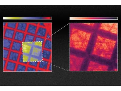
Photo: Researchers at MIT have shown how one could improve the efficiency of scintillators by at least tenfold by changing the material’s surface. This image shows a TEM grid on scotch tape, with the right side showing the scene after it is corrected. Credit: Image courtesy of Charles Roques-Carmes, Nicholas Rivera, Marin Soljacic, Steven Johnson, and John Joannopoulos, et al