Nanofabrication, or self-assembly, of materials offers new possibilities in the development of catalysts, batteries, photonics devices and more. One major barrier to taking full advantage of nanofabrication, and tuning the nanoscale assembly process, is the difficulty in seeing beyond the surface of 3D nanostructures in order to view the positions of individual particles and identify any imperfections. Researchers from the Columbia University School of Engineering and Applied Science, along with the U.S. Department of Energy’s Brookhaven National Laboratory and its Center for Functional Nanomaterials (CFN), have now achieved unprecedented resolution using a hard X-ray beamline at the National Synchrotron Light Source II (NLS-II), providing a highly detailed view inside nanoparticle lattices to help guide improvements for assembling new materials.
The team designed nanoscale materials using DNA as a programmable construction material to arrange thousands of nanoparticles into a superstructure based on a template designed by the researchers. The engineered materials have potential applications in catalysis, optics and withstanding extreme environments, and the resulting self-assembled 3D lattices came to a size of about 2 micrometers. One of the challenges of seeing within these tiny structures is the destructive effect X-rays have on the DNA-nanoparticle samples, so the Columbia and CFN researchers used precise nanoscale inorganic templating methods to produce inorganic replicas of their 3D nanostructures, which can withstand powerful X-rays. The other challenge was tuning the Hard X-ray Nanoprobe (HXN) beamline at NSLS-II to achieve the necessary improvements in resolution, data acquisition and more, that would allow individual particles in the structure to be viewed in 3D. Through gradual progress, with speed and data acquisition improving with each attempt, the team came to the point where a full data set could be achieved in just one day, said first author Noam Michelson.
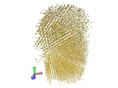
The researchers leveraged the HXN beamline by measuring both the phase contrast of the X-rays passing through the samples and the X-ray fluorescence from the sample during analysis. They also developed new software tools to process the large amount of data obtained, and used both standard analysis and machine-learning approaches to validate the resolution they achieved. Ultimately, the researchers were able to determine the positions of about 10,000 individual nanoparticles within a lattice, with a resolution of just 7 nm. With this information, the team could precisely assess the arrangements of assembly motifs as well as identify any defects and imperfections in the assembly. These insights can allow the researchers to better tune and control the fabrication process and identify areas for improvement in their design. This research was published in Science.
“Measuring the data was only half the battle; now we needed to translate the data into meaningful information about order and imperfection of self-assembled systems. We wanted to understand what type of defects can occur in these systems and what is their origin,” explained co-corresponding author Oleg Gang. “Until this point, this information was only available through computation. Now we can really see this experimentally, which is super exciting and, literally, eye-opening for the future development of complex designed nanomaterials.”
Now, the team plans to further investigate the relationships between the defects observed and the properties of their materials, and work toward a new bottom-up nanofabrication platform that can be imaged using the improved methods, said Gang. Researchers also plan to further improve the beamline to allow for even faster data acquisition in the future, said co-corresponding author Hanfei Yan, a beamline scientist at HXN.
Photo: Reconstructed nanoparticle lattices; every golden dot represents one of the nanoparticles in the assembled structure. Credit: Oleg Gang/Columbia Engineering