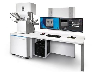
The TESCAN SOLARIS 2 is designed for fully automated TEM lamella preparation using the AI-powered TESCAN TEM AutoPrep Pro software. The system produces high-quality, ultra-thin samples for sub-10 nm technology nodes, such as advanced logic and memory devices. AI-driven precision delivers high-quality samples with minimal damage, supporting various geometries such as top-down, planar, and inverted lamellae. The automated workflows reduce setup time and optimize system readiness, ensuring productivity for users at all experience levels.
Meanwhile, the TESCAN SOLARIS X 2 extends the capabilities of physical failure analysis with its Mistral Xe Plasma FIB column, providing large-area cross-sectioning and gallium-free TEM lamella preparation for complex semiconductor packages, including 2.5D, 3D IC, and MEMS devices. The Triglav SEM column enables nanometer-level accuracy for defect isolation in advanced semiconductor packaging.
Lastly, the TESCAN AMBER X 2 provides precision delayering with uniform, artifact-free results, supporting sub-10 nm technology nodes. This system is built for electrical failure analysis, allowing in-situ verification through SEM-based nanoprobing and efficient defect isolation. Researchers can achieve consistent results with tailored gas chemistries like Nanoflat Chase and C-maze, optimized for NMOS and PMOS transistors.
These systems are built to address the growing complexities of modern semiconductor technologies, improving the efficiency and accuracy of failure analysis for researchers and engineers.