Featured Article
Please check out our Microscopy and Laboratory Microscopes section for more information or to find manufacturers that sell these products.
In the 1980s, Sun
Microsystems coined
the trademark “The
Network is the Computer”
to herald the days
of distributed computing.
National Instruments
(Austin, TX), purveyors of the popular Lab-
VIEW™ instrumentation programming
environment, built on the meme, trademarking
“The Software is the Instrument” to
signal the dawn of virtual instrumentation.
Today, microscopy’s vanguard has charged
beyond the realm of Abbe, Nachet, Janssen,
and the other originators of the field.1 Automated
image acquisition and reconstruction,
clever optical strategies, intensive databasing
and analysis, and resolutions below the Rayleigh
criterion are the new frontiers,2 with
early settlements emerging in the form of
imaging suites crafted by pioneering technologists
(Table 1). Increasingly, the imaging
suite is the microscope.
Software, the driver
Thus commences the next phase of the laboratory’s
personal computer revolution, first
spotlighted in American Laboratory in annual
purchasing surveys in the mid-1980s when the
personal computer became the largest laboratory
budget category for the first time. Today,
imaging suites that control the microscope, camera, focusing mechanism, and sample
positioning stages do not just serve the microscope—
They define its capabilities and that
of the application, and the suites are growing
increasingly vertical in their focus. Examples
include Metamorph and MetaFluor (Molecular
Devices, Sunnyvale, CA), μManager
(Vale Laboratory, University of California at
San Francisco), ScanImage
(HHMI Janelia
Farm, Ashburn, VA), and SlideBook™ suite
(Intelligent Imaging Innovations, Denver,
CO), all of which support an impressive array
of hardware from manufacturers committed to
users’ quick productivity.
This has increased market awareness of software
as not only an enabler for industrial and
academic research, but also as a pacing item
for instrumentation manufacturers. Generally
speaking, microscopy users must prioritize
quick productivity and ease of use; thus lowlevel
connectivity of the instrumentation is
of little utility outside of the most exotic hinterlands
of the field, such as single-molecule
biophysics, where each setup is still unique
and researchers are developing the foundations
of tomorrow’s platforms and writing
their own code. Instead, the majority of
today’s microscopy applications are increasingly
well-served by imaging suites that
offer plug-and-play support of popular subsystems,
and microscope manufacturers and
distributors offer configuration services (and
sometimes their own proprietary platforms)
that allow users to devote their attention to
their real work. In this way, subsystems have
taken on a role reminiscent of common office
peripherals like printers and scanners: Users
expect them to “just work” without a lot of
low-level engineering on their part.
High hurdles for manufacturers
and innovative responses
The challenge for subsystem manufacturers
is how to support both this expanding
mainstream of sophisticated applications
suites, with their plug-and-play prerogative,
and the engineers and scientists
immersed in developing tomorrow’s techniques
and writing their own code. At the
same time, subsystem manufacturers must
keep pace with the increasing importance
of high-speed acquisition and processing.
This has driven a cascade of developments
that have included:
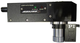
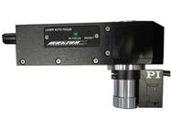
Figure 1- Laser autofocus sensor with fast
piezo focus positioner and objective (courtesy of PI
[Physik Instruments] L.P. [San Jose, CA] and
Motion X Corp. [Santa Barbara, CA]).
- Advancedinter-face techniques that
of fer microsecondscale
synchronization
between motion and
optical processes
- Novel motion devices
with extended travels,
resolution capabilities and stabilities,
new sensors, and command sets with
backward and forward compatibility as
new controls are developed
- Digital nanopositioning controllers of
extraordinary capability but that undercut
traditional analog controls in price
due to semiconductor developments
- Innovative control techniques that
address fundamental limitations in
motion system bandwidths, for more
accurate scanning and acquisition.
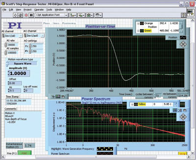
Figure 2 - Sixy-millisecond capture of focus demonstrated
by laser vibrometer independently measuring
PIFOC® piezo objective scanner (PI) position vs time.
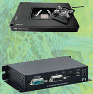
Figure 3 - The valuetrend enjoyed by consumers
has now evolved to nanopositioning, with the introduction
of cost-effective digital controllers for a fraction
of their former price and which support popular
imaging suites. XYZ piezo stage for super resolution
(SR) microscopy is shown in the background.
For example, the need for precise focusing
mechanisms (either piezo objective positioners
or piezo Z scanning stages) to instantly acquire
focus and keep it locked in despite structural
drifts and specimen motions has outstripped the
capabilities of previous-generation
probe-based
sensors that could compensate for only some
drift mechanisms. The industry has responded
with both image- and sensor-based autofocus
approaches that meet these emerging needs
and that leverage sophisticated new interfacing
capabilities. In particular, laser autofocus sensors
coupled with fast nanopositioning controllers
can now acquire and lock in perfect focus in
milliseconds, even starting from many hundreds
of microns out of focus (see Figures 1 and 2).
Similarly, the need for high applications
throughput has also driven the demand for
larger-area scanning capabilities for sample
positioning stages. In turn, these new
requirements for fast motions place a premium
on coarse-positioning stage stiffness
and stability. The industry’s response has
been to develop new types of drives that
eliminate the primary drift mechanism of
common microscopy substages.3 Meanwhile,
the skyrocketing functionality-tocost
ratio of modern microelectronics has seen the introduction of digital nanopositioning controllers at a fraction of the former
cost of such instruments (see Figure 3).
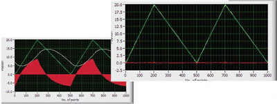
Figure 4 - Dynamic Digital Linearization
(DDL) (PI) is an in-controller technology for
eliminating following errors (red). Green: commanded,
white: actual, red: following error. Left:
without DDL; right: with DDL. The green and
white traces are indistinguishable
Tomorrow’s imaging applications are growing,
some leveraging optical tweezers and
atomic force probes to image almost
unimaginably small structures. These
applications depend on the utmost in
instrumentation performance and interfacing
capabilities.4 Applications are
just starting to take full advantage of
advanced technologies such as the ability
of some nanopositioning controllers
to virtually eliminate the following
error present in rapid actuation. This
allows faster scanning without loss of
localization accuracy (see Figure 4).
An exciting future
The mash-up of advanced optics, novel
illumination and fluorescence techniques,
new sensors, and advanced nanopositioning
subsystems is just beginning to unfold.
At the same time, the promise of automating
sophisticated setups to leverage the
speed, analytical power, and data handling
prowess of today’s computers and software
architectures is just beginning to be realized. It
is safe to say that the microscopy of 2035 will
bear as much resemblance to today’s microscopy
as a personal computer bears to the first
PCs that topped the American Laboratory budget
surveys just 25 years ago.
Please check out our Microscopy and Laboratory Microscopes section for more information or to find manufacturers that sell these products.
References
- Parmentier, J. The History of the Microscope—
An Introduction to Microscopy; www.microscopy-uk.org.uk/intro/histo.html.
- Geisler, C. Dissertation—Fluorescence
nanoscopy in three dimensions; http://webdoc.sub.gwdg.de/diss/2010/geisler/geisler.pdf.
- Jordan, S.; Anthony, P. Design considerations
for micro- and nanopositioning:
leveraging the latest for biophysical application.
Curr. Pharm. Biotechnol. 2009, 10,
515–21; www.bentham.org/cpb/sample/cpb10-5/0008G[1].pdf
- Churnside, A.B.; King, G.M. et al. Improved
performance of an ultrastable measurement
platform using a field-programmable gate
array for real-time deterministic control. In
Instrumentation, Metrology, and Standards for
Nanomanufacturing II; Postek, M.T.; Allgair,
J.A., Eds. Proceedings of the SPIE, 2008, Vol.
7042, pp704205-704205-7.
Mr. Jordan is Director, NanoAutomation™ Technologies,
PI (Physik Instrumente) L.P., 6537
Fall River Dr., San Jose, CA 95120, U.S.A.;
tel.: 949-679-9191;fax: 949-679-9292; e-mail: [email protected].