New Stylus Profiler Enables Semi-Automated Measurements with Uncompromised 300mm Access
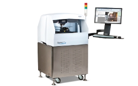
BILLERICA, Mass. – January 14, 2014 – Bruker (NASDAQ: BRKR) today announced the release of the Dektak XTL Stylus Profiler, extending its industry-leading stylus profilometry capabilities to 200 and 300 millimeter semiconductor wafer fabs and next-generation touch panel manufacturers. The system provides the most cost-effective, full 300-millimeter wafer solution for characterizing thin film step heights, resist step heights, line edge roughness, CMP dishing and erosion, as well as roll off amount (ROA). The Dektak XTL combines decades of stylus innovation with new features targeting QA/QC environments to enable increased accuracy and minimal operator intervention between loading and unloading samples.
“Bruker’s Dektak XTL with a 12-inch stage is the most advanced system in its class,” said Roger Lee, Integration Department Project Director for China Wafer Level CSP Co., Ltd. (WLCSP). “The system is stable and reliable, and it incorporates many powerful functionalities and ease-of-use features. Bruker’s stylus profilers always lead the industry in technology, and they always meet our metrology requirements in production.”
“Customers like WLCSP have been asking for a larger scale stylus measurement system to support their latest 300mm wafer factory needs with the accuracy and industry-proven repeatability of our traditional Dektak products,” added Kent Heath, General Manager of Bruker’s Stylus and Optical Metrology business unit. “With the Dektak XTL we have delivered on this need with its 5 nanometer repeatability, and we have built-in a new level of point-and-click automation for maximum productivity that is unrivaled in the industry. Our early access customers have been amazed by how intuitive it is to use for production and development applications.”
About Dektak XTL
The Dektak XTL features a small footprint with pneumatic passive isolation and a fully enclosed workstation with a wide, easily accessible interlocking door, making it suitable for demanding production floor environments. Its dual-camera architecture enables enhanced spatial awareness, and its high level of automation maximizes manufacturing throughput. Bruker’s exclusive Vision64® Advanced Production Interface (API) with pattern recognition optimizes the system for stringent QA/QC requirements and makes data collection an intuitive and repeatable process, minimizing operator-to-operator variability.
About Bruker Corporation (NASDAQ: BRKR)
Bruker Corporation is a leading provider of high-performance scientific instruments and solutions for molecular and materials research, as well as for industrial, diagnostics and applied analysis. For more information about Bruker Corporation, visit www.bruker.com.
Media Contact:
Stephen Hopkins, Marketing Communications
Bruker Nano Surfaces Division
T: +1 (520) 741-1044 x1022
E: [email protected]
Investor Contact:
Joshua Young
Bruker Corp.
T: +1 (978) 663-3660 x1479
E: [email protected]