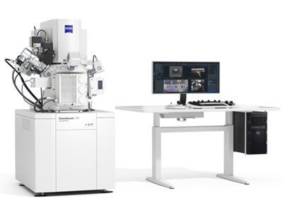
The new ZEISS Crossbeam 550 Samplefab is a focused ion beam scanning electron microscope (FIB-SEM) optimized for fully automated preparation of transmission electron microscopy (TEM) samples (lamellae).
Built for efficiency and throughput in the semiconductor lab, ZEISS Crossbeam 550 Samplefab provides recipe-based automation for the routine TEM sample preparation work of bulk milling, lift-out and thinning at any number of target points on the sample. The solution promises an automation yield of >90% for processing lamellae from bulk to TEM grid without operator intervention. Automated checks allow human interventions to ensure no lamellae are lost during processing, driving lamella success rates towards 100%.
TEM imaging provides essential information for understanding semiconductor device defects and improving process yield. However, the accuracy of the data from TEM analysis is dependent upon producing high-quality lamellae accurately, repeatedly and with high throughput.
ZEISS Crossbeam 550 Samplefab uses the Gemini 2 electron column, allowing the operator to observe the sample live with the SEM during FIB milling to achieve the highest final lamella quality and endpointing outcomes when thinner samples are required than what is provided by the automation.